Abstract
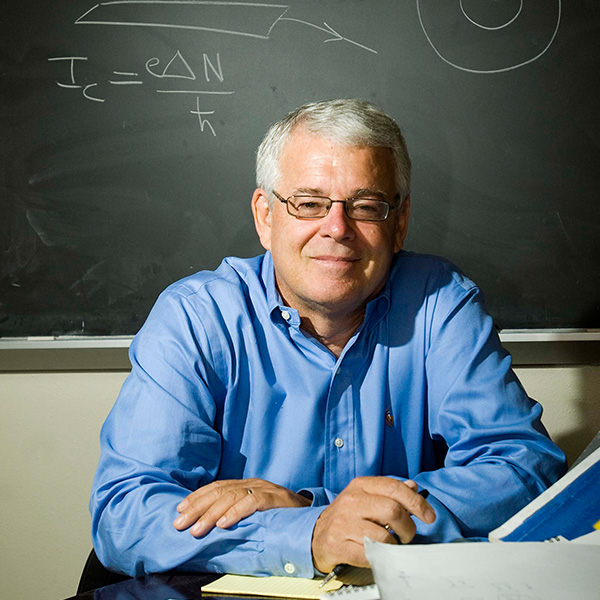
Moiré superlattices of 2D materials is an emerging platform for studying new physical phenomena with high tunablity. In this talk, I will present emergent magnetic interactions in two distinct types of moiré superlattices. I will firstly present the observation of magnetic textures in small angle twisted 2D magnet chromium triiodide (CrI3). Employing single-spin quantum magnetometry, we directly visualize nanoscale magnetic domains and periodic patterns, a signature of moiré magnetism, and gain quantitative information on domain size and magnetization. The observed AFM and FM domains with periodic patterns are in good agreement with the calculated spatial magnetic structures arising from the local stacking-dependent interlayer exchange interactions in CrI3 moiré superlattices. Then I will present the drastic tuning of spin-spin exchange interactions in WSe2/WS2 moiré superlattices by optical excitation, which results in ferromagnetic order over a small range of doping at elevated temperatures. This discovery adds a new and dynamic tuning knob to the rich many-body Hamiltonian of moiré quantum matter.
Biography
Prof. Xiaodong Xu is a Boeing Distinguished Professor in the Department of Physics and the Department of Materials Science and Engineering at the University of Washington. Prof. Xu received his PhD (Physics, 2008) from the University of Michigan and then performed postdoctoral research (2009-2010) at the Center for Nanoscale Systems at Cornell University. His nanoscale quantum optoelectronics group at University of Washington focuses on creation, control, and understanding of novel device physics based on two-dimensional quantum materials.
Abstract
Supersolid, an elusive state of matter that is both solid- and superfluid-like, has evaded experimental detection for decades until its recent discovery in cold atom experiments. The emergence of moiré materials presents a new platform to realize supersolids in solid-state materials. In this talk, I will first discuss how to create an equilibrium exciton fluid in Coulomb-coupled moiré double layers by controlling the relative interlayer concentration of electrons. I will then discuss how to utilize the exciton-electron repulsion in a Bose-Fermi mixture to realize an excitonic density wave: An exciton fluid that spontaneously breaks the translational symmetry of the moiré lattice. The new state of matter promises future detection of excitonic supersolidity.
Biography
Prof. Kin Fai Mak received his PhD in physics from Columbia University working with Prof. Tony Heinz on optical spectroscopy of 2D materials such as graphene and MoS2. As a postdoc, he worked with Prof. Paul McEuen and Prof. Jiwoong Park at Cornell on the optoelectronic properties of 2D semiconductors. They have demonstrated the valley Hall effect in MoS2 transistors using optoelectronics methods. Prof. Mak started his faculty position at Penn State University in 2014 and moved back to Cornell in 2018. He is now an associate professor of physics and of applied and engineering physics. Prof. Mak is interested in many topics in condensed matter physics. His current research interests include magnetism, superconductivity, strong correlation physics and excitonic physics in 2D materials and their heterostructures.
Abstract
Transition metal dichalcogenides (TMDs) have become an exciting platform to explore optoelectronics with the appealing optical properties of tightly bound excitons formed in the degenerate valleys at Brillouin zone corners. In this talk, I will introduce two schemes to realize chiral light-matter interfaces respectively for valley excitons in monolayer, and for dipolar valley excitons in double layer, which can be exploited for optical injection of unidirectional exciton flow. Placing monolayer on periodically structured dielectric substrate, we find the spatial modulation of the Coulomb interaction can lead to the formation of exciton Bloch states with real-space valley pseudospin texture displayed in a mesoscopic supercell, pattern-locked to the propagation direction [1]. This enables nano-optical excitation of unidirectional exciton flow through the valley selection rule, with the angular directionality controlled by the excitation location, exhibiting a vortex pattern in a supercell. For dipolar valley excitons in twisted double layer TMDs, we show that either in-plane magnetic field or heterostrain can induce a sizable multiplet splitting inside the light cone, where the chiral dispersions of the split branches make possible efficient optical injection of unidirectional exciton current [2]. Angular orientation of photo-injected exciton flow can be controlled by strain or field direction, with left-right unidirectionality selected by circular polarisation. These point to new opportunities for excitonic devices with non-reciprocal functionalities.
The works are supported by the Research Grant Council of Hong Kong SAR (AoE/P-701/20, HKU SRFS2122-7S05), and the Croucher Senior Research Fellowship.
[1] Xu-Chen Yang, Hongyi Yu and Wang Yao, Chiral excitonics in monolayer semiconductors on patterned dielectric, arXiv:2110.07642.
[2] Huiyuan Zheng, Dawei Zhai, and Wang Yao, Anomalous magneto optical response and chiral interface of dipolar excitons at twisted valleys, submitted.
Biography
Prof. Wang YAO obtained his BSc from Peking University in 2001, and PhD in physics from University of California, San Diego in 2006. He joined the University of Hong Kong in September 2008, and is currently Chair Professor in the Department of Physics. His research interest lies in the physics of spin and valley in solids, with a current focus on two-dimensional materials and their heterostructures. He has received honours including the OCPA Achievement in Asia Award (Robert T. Poe Prize), Croucher Innovation Award, Nishina Asia Award, XPlorer Prize, and has been named by Clarivate Analytics in the list of "Highly Cited Researchers" in consecutive years from 2018 to 2021. In 2020, he is elected Fellow of American Physical Society.
Abstract
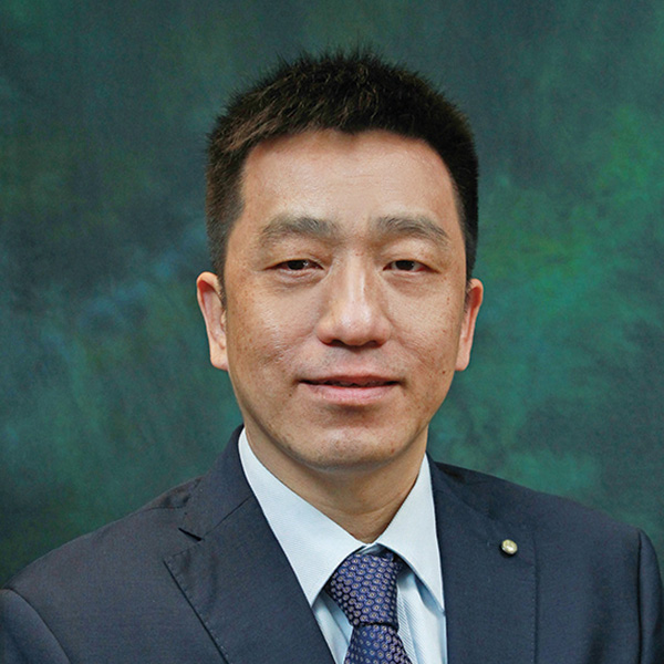
Research on two-dimensional (2D) materials and relevant synthesis techniques is curently an important cutting-edge field in materials science. Particularly, 2D materials provide opportunities for developing semiconductor applications at atomistic thickness to break the limits of existing integrated circuit technology. Black phosphorus (BP), as a layered 2D semiconductor with controllable bandgap and high carrier mobility, is one of the most promising candidates for transistor devices at atomistic thickness. However, the lack of large-scale growth greatly hinders its development in devices. In this talk, I will introduce our recent progress on the growth of ultrathin BP on the centimetre scale through pulsed laser deposition (PLD). In this work published in Nature Materials (2021), we present a controllable and rapid PLD process to directly synthesize few-layered BP with high crystallinity and homogeneity. Furthermore, we made advances by fabricating BP-film-based centimetre-scale field-effect transistor (FET) arrays that exhibit appealing electrical performances. In addition to the growth of BP, PLD is particularly attractive for making some specific 2D materials and vdW heterostructures, including Bi, InSe and lanthanide-doped TMDCs obtained in our results. Our works imply that that PLD will be useful for electronic, magnetic and photonic device applications based on various 2D materials and heterostructures.
Biography
Prof. Jianhua Hao is currently a Chair Professor of Materials Physics and Devices in PolyU. He has published 340 internatioanl journal papers, including Nature, Nature Materials, Nature Commun., Adv. Mater., JACS, ACIE, Adv. Energy Mater., ACS Nano, Phys. Rev. Lett. and Nano Lett.. He has been PC/PI in 20+ external grants, including 1 RGC CRF COVID-19 as PC, 14 RGC GRF (10 in a row since 2012/2013), 3 ITF and 3 NSFC. He received "Natural Science Award by the Ministry of Education", “TechConnect Global Innovation Award”, “Special Merit Award and Gold Medal of Geneva”, and PolyU President’s Award. He serves as Associate Editor of InfoMat (Wiley, IF~25.405) and Editorial Board Member of international journals (Advanced Optical Materials, etc.). He is conferred as RGC Senior Research Fellow, and elected as Fellow of the Optical Society, Fellow of Royal Society of Chemistry, and Fellow of Institute of Physics. His research focuses on (1) Functional thin-films, 2D materials and heterostructures; (2) Luminescence and phosphors for photonic, biomedical and nano energy applications.

Abstract
Layered two-dimensional (2D) platinum dichalcogenides, such as PtSe2 and PtS2, have received significant interest due to their potential applications in many fields, including electronics, optoelectronics, electrochemical hydrogen production, and so on. A layer-dependent semiconductor-to-semimetal evolution of 2D layered PtSe2 is revealed. The few-layer PtSe2 field-effect transistor shows high room-temperature mobility (≈210 cm2V−1s−1) in a back-gated configuration on SiO2/Si, comparable to BP. A facile strategy is reported to synthesize large-area and edge-rich PtSe2 via selenization of Pt films. The edge site density of the PtSe2 can be effectively controlled by tuning the thickness of Pt films. A high-performance photodetector based on PtTe2/Si Schottky junction can sense ultra-broadband light of up to 10.6 μm with a high specific detectivity. The MIR surface plasmons in the PtTe2 were observed by near-field nanoimaging. Furthermore, despite its semimetallic nature, PtSe2 could support dielectric waveguide modes in MIR.
Biography
Prof. Daniel Lau is a Chair Professor of Nanomaterials in Department of Applied Physics at the Hong Kong Polytechnic University. He has been the Head of the Department since 2013. Prof. Lau is a Fellow of the American Physical Society. His current research focuses on two-dimensional (2D) materials and energy materials, particularly the synthesis of 2D materials for optoelectronic, electrocatalysis, and energy storage applications.

Abstract
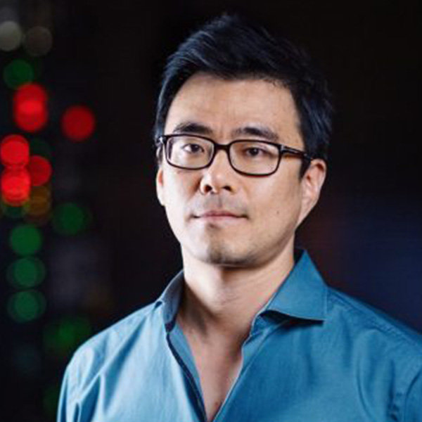
2D material-based devices have received great deal of attention as they can be easily stacked to obtain multifunctionality. With their ultrathin thicknesses, such multifunctioning devices become so flexible and conformal that they can be placed onto any 3D featured surfaces. However, 2D heterostructures are typically demonstrated as stacked flakes where single or few devices can be fabricated due to lack of strategies for layer-by-layer stacking of 2D materials at the wafer scale. In this talk, I will discuss about our unique strategy to isolate wafer-scale 2D materials into monolayers and stack them into a heterostructures by using a layer-resolved splitting (LRS) technique [1]. This technique enables my group at MIT to explore unprecedented wafer-scale 2D heterodevices including integrated photonics, 3D neuromorphic computing, and microLEDs, which will be introduced in my talk.
While 2D heterostructures promise interesting futuristic devices, the performance of 2D material-based devices is substantially inferior to that of conventional 3D semiconductor materials. However, 3D materials exist as their bulk form, thus it is challenging to stack them together for heterostructures. Obviously, conformal coating of such single-crystalline bulks on 3D features is impossible. My group at MIT has recently invented a 2D materials-based layer transfer (2DLT) technique that can produce single-crystalline freestanding membranes from any compound materials with their excellent semiconducting performance [2-4]. This technique is based on remote epitaxy of single-crystalline films on graphene followed by peeling from graphene. Stacking of freestanding 3D material membranes will enable unprecedented 3D heterostructures whose performance is expected to be superior to that of 2D heterostructures. I will talk about our group’s effort to apply single-crystalline freestanding membranes for flexible, conformal electronics as well as for 3D heterostructures.
Finally, I will conclude my talk by discussing perspectives of coupling 2D-3D freestanding membranes for 2D-3D mixed heterostructured devices that can be enabled by our LRS and 2DLT techniques [5,6].
References
[1] J. Shim, S. Bae, et al, and J. Kim, “Controlled crack propagation for atomic precision handling of wafer-scale two-dimensional materials” Science, 362, 665 (2018)
[2] Y. Kim, et al, and J. Kim, “Remote epitaxy through graphene enables two-dimensional material based layer transfer” Nature, Vol. 544, 340 (2017)
[3] W. Kong, et al, and J. Kim, “Polarity govern atomic interaction through two-dimensional materials”, Nature Materials, Vol. 17, 999 (2018)
[4] S. Bae et al, and J. Kim, “Graphene-assisted spontaneous relaxation towards dislocation-free heteroepitaxy”, Nature Nanotechnology, published online (2020)
[5] S. Bae, et al, and J. Kim, “Integration of bulk materials with two-dimensional materials for physical coupling and applications”, Nature Materials (2019)
[6] H. Kum, et al., and J. Kim, “Heterogeneous integration of singlecrystalline complex-oxide membranes, Nature, Vol 578, 75-81 (2020)
Biography
Prof. Jeehwan Kim's group at MIT focuses on innovations in nanotechnology for next generation computing and electronics. Prof. Kim joined MIT in September 2015. Before joining MIT, he was a Research Staff Member at IBM T.J. Watson Research Center in Yorktown Heights, NY since 2008 right after his Ph.D. He worked on next generation CMOS and energy materials/devices at IBM. Prof. Kim is a recipient of 20 IBM high value invention achievement awards. In 2012, he was appointed a “Master Inventor” of IBM in recognition of his active intellectual property generation and commercialization of his research. After joining MIT, he continuously worked nanotechnology for advanced electronics/photonics. As its recognition, he received LAM Research foundation Award, IBM Faculty Award, DARPA Young Faculty Award, and DARPA Director’s Fellowship. He is an inventor of > 200 issued/pending US patents and an author of > 50 articles in peer-reviewed journals. He currently serves as Associate Editor of Science Advances, AAAS. He received his B.S. from Hongik University, his M.S. from Seoul National University, and his Ph.D. from UCLA, all of them in Materials Science.
Abstract
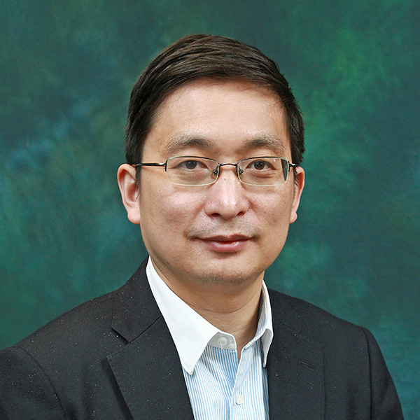
As the Moore’s Law is anticipated to flatten in the near term, it requires an investment in both basic sciences (including materials science) and computation paradigms to foster continued technology development in microelectronics. Two-dimensional (2D) layered semiconductors possess atomic level thickness, dangling-bond-free surface and unique physics, promising their potentials for post-Moore’s law computing.
More Moore: Ultrathin 2D semiconductors provide potential for downward scaling to nanoscale and low-power transistors. However, their dangling bond–free surface makes it extremely difficult to deposit gate dielectrics with high-quality interface in metal-oxide-semiconductor (MOS) field-effect transistors (FETs). We demonstrate a low-temperature process to transfer metal gate to 2D MoS2 for high-quality interface. The high–barrier height Pt-MoS2 Schottky junction replaces the commonly used MOS capacitor and eliminates the use of gate dielectrics, exhibiting sub-1 V operation voltage and a subthreshold slope close to thermal limit (60 mV/dec) and enabling logic functions in a single transistor with small footprint. [1]
More than Moore: The number of nodes typically used in sensory networks is growing rapidly, leading to large amounts of redundant data being exchanged between sensory terminals and computation units. To efficiently process such large amounts of data, it is necessary to develop approaches to computing that operate close to or inside sensory networks, and that can reduce the redundant data movement between sensing and processing units. [2] We demonstrate bioinspired in-sensor vision adaptation sensors that are based on MoS2 phototransistors and exhibit time-varying activation and inhibition characteristics. The approach offers in-sensor visual adaptation with highly localized and dynamic modulation of photosensitivity under different lighting conditions at the pixel level, creating an effective perception range of up to 199 dB and showing both scotopic and photopic adaptation. [3]
[1] Science Advances, 2021, 7: eabf8744.
[2] Nature Electronics, 2020, 3, 664-671.
[3] Nature Electronics, 2022, 5, 84-91.
Biography
Dr Yang Chai is an Assistant Dean of Faculty of Applied Science and Textile of the Hong Kong Polytechnic University, Vice President of Physical Society of Hong Kong, a member of The Hong Kong Young Academy of Sciences, an IEEE Distinguished Lecturer since 2016, and was the Chair of IEEE ED/SSC Hong Kong Chapter (2017-2019). He is a recipient of RGC Early Career Award in 2014, the Semiconductor Science and Technology Early Career Research Award in 2017, PolyU FAST Faculty Award in Research and Scholar Activities in 2018/2019, Young Scientist Award of ICON-2DMAT in 2019, PolyU President’s Award in Research and Scholar Activities in 2019/2020, NR45 Young Innovators Award in 2021, and Young Scientist of World Laureate Forum in 2021. His current research interest mainly focuses on emerging electronic devices.
Abstract
In this paper, we addressed this challenge by applying the asymmetric elastoplasticity of stacked graphene assembly (SGA) under tension and compression. In particular, we transferred the SGA onto a polyethylene (PE) film, the resulting SGA/PE bilayer exhibits swift morphing behavior of the bilayer materials in response to the variation of the surrounding temperature. Moreover, with the application of patterned SGA and/or localized tempering pretreatment, the initial configurations of such thermal-induced morphing systems can also be programmed as needed, enabling the creation of a variety of actuation systems with sophisticated three-dimensional structures. More importantly, different from normal bilayer actuators, the SGA/PE bi-material, after tempering-like heat treatment in a constrained space, can spontaneously curl into a roll, which even achieves rolling locomotion under lateral infrared lighting, yielding an untethered light-driven motor. The asymmetric elastoplasticity of SGA endows the SGA/PE bi-materials with great application potential in actuators, motors, and untethered soft robotics with high programmability.
Biography
Dr. Haimin Yao is an Associate Professor at the Hong Kong Polytechnic University. He received his BEng and MEng degrees from Tsinghua University in 2000 and 2002 respectively, and Doctor degree from Universität Stuttgart, Germany in 2006. Dr. Yao’s research interest focuses on the mechanical behaviors of solid materials including biological materials, energy materials, and two-dimensional materials.

Abstract
The past several decades have witnessed tremendous interests and studies in low dimensional materials, such as 1D or 2D materials. They have attracted significant attention owing to their unique structures, remarkable properties, and great potential for a wide range of applications in electronics, optoeletronics, valleytronics, catalysis, etc. Chemical vapor deposition (CVD) method has been widely investigated to synthesis these materials in large area (wafer scale) and good quality. In this talk I will present our recent work on their synthesis and integration. As monolayer semiconductors are promising for future electronics, I will also present our recent progress to achieve reliable low contact resistance for n-type 2D semiconductors.
Biography
Prof. Jing Kong received her B.S degree in Chemistry from Peking University, Beijing, China in 1997 and PhD degree in Chemistry from Stanford University in the United States, 2002. In 2004, she joined the faculty at MIT, where she is currently Professor in the Electrical Engineering and Computer Science Department. She has worked in the field of carbon nanotubes since 1997 and has published numerous papers on this subject. In MIT this research lead to the synthesis of related nanostructures such as graphene and later graphene-like two dimensional materials. The current research activity in her group involves CVD synthesis, characterization of these low dimensional materials, investigation of their electronic and optical properties and developing their applications.
Abstract
Modern information technologies require large performance improvements in integrated circuit systems. Two approaches, including lateral scaling and vertical scaling, are being developed to advance the performance of solid-state electronics. The talk shall focus on how to use two-dimensional materials for both directions.
(1) Continue the transistor lateral scaling (Moore’s Law). With the scaling for future technology nodes, the gate controllability becomes weaker owing to the pronounced source-drain tunneling. Hence, the transistor body thickness needs to be reduced to ensure efficient electrostatic control. Thin materials with perfect surfaces such as transition metal dichalcogenide (TMD) monolayers offer a great chance to continue the scaling. Possible solutions for major challenges at a device level such as materials selection, materials growth, metal contact, and scaling of gate dielectric thickness, will be discussed.
(2) Vertical scaling: monolithic 3D integration. 3D monolithic integration, such as adding sensor functionalities, constructing upper-layer logic circuits or memory devices on CMOS Si wafers, or stacking logic with memory devices, is anticipated to save the footprint and power consumption of chips. Transistors based on 2D materials is a low-power device that can be integrated monolithically. The central topic is to develop the materials and processes compatible with the backend-of-line (BOEL) fabrication temperature.
Biography
Prof. Lance Li has been the Chair Professor of Future Electronics at the University of Hong Kong (HKU) since 2021 with the research focus on solving grand challenges in using low-dimensional materials for scaled electronics and as backend transistors for monolithic 3D integration.
Prior to joining HKU, Prof. Li was a Director of Corporate Research in Taiwan Semiconductor Manufacturing Company (TSMC) from 2017 to 2020. He was working on developing key technologies of integrating low-dimensional materials with current micro/nanoelectronics.
Prof. Li worked as a Professor at KAUST from 2014-2017, a research fellow at Academia Sinica in Taiwan (2010-2014), an Assistant Professor at Nanyang Technological University (NTU) Singapore (2006-2009) respectively. He received his PhD in condensed matter physics at Oxford University, and MSc/BSc degrees in Chemistry at National Taiwan University. He is a highly cited scholar since 2018.
Abstract
Nature Materials offers authors high visibility for their work. A team of full-time, professional editors select and commission articles that represent a substantial and arresting fundamental, mechanistic, methodological or practical advance. In this talk I will convey the editor’s perspective on the life of a manuscript after submission to Nature Materials, and provide an overview of the types of content that we publish.
Biography
Dr Daniel McNally received a BSc in Physics and Astrophysics from University College Cork and a MSc in Physics from Trinity College Dublin in Ireland. He earned his PhD in Physics at Stony Brook University and Brookhaven National Laboratory focusing on strongly correlated materials, with a particular emphasis on neutron scattering. He continued to work on quantum materials using resonant inelastic x-ray scattering as a postdoctoral researcher at the Paul Scherrer Institut, Switzerland. At Nature Materials, which he joined in March 2018, Dr McNally handles manuscripts in correlated electron systems, topological materials and spintronics. Dr McNally is currently based in the New York office.
Abstract
Two-dimensional (2D) layered materials have been an exciting frontier for exploring emerging physics at reduced dimensionality. There has been exciting progress in discovering 2D structures/phases with various functionalities, including ferromagnetism, superconductivity, piezoelectricity and ferroelectricity, offering a wealth of choices to make 2D heterostructure devices. One of the examples has been the demonstration of room-temperature 2D ferroelectric materials such as CuInP2S6, MoTe2, WTe2 and In2Se3, promising for making ultrathin flexible ferroelectric devices. While exploring the 2D ferroelectricity in vdW In2Se3, we discovered a novel 2D antiferroelectric phase competing with the ferroelectric phase, using optical and electron microscopy consolidated by first-principles calculations[1]. Different from conventional 3D antiferroelectricity, antiferroelectricity in In2Se3 is confined within the 2D layer and generates the unusual nano-stripe ordering: the individual nano-stripes exhibit local ferroelectric polarization, whereas the neighboring nano-stripes are antipolar with zero net polarization. Such a unique superstructure is underpinned by the intriguing competition between 2D ferroelectric and antiferroelectric ordering in In2Se3, the balance of which determines the nano-stripe width. Fascinatingly, we also unveil 2D ferroelasticity coupled with this antiferroelectric superstructure through the spontaneous lattice strain[2]. Both the observed antiferroelectricity and ferroelasticity can be preserved down to single-layer thickness, as predicted by calculation, further enriching the 2D functionality choices for ultrathin device fabrication.
[1] C. Xu, Y. Chen, X. Cai, A. Meingast, X. Guo, F. Wang, Z. Lin, T.-W. Lo, C. Maunders, S. Lazar, N. Wang, D. Lei, Y. Chai, T. Zhai, X. Luo, Y. Zhu* “Two-dimensional antiferroelectricity in nanostripe-ordered In2Se3” Phys. Rev. Lett. 125, 047601 (2020).
[2] C. Xu, J. Mao, X. Guo, S. Yan, Y. Chen, T.W. Lo, C. Chen, D. Lei, X. Luo, J. Hao, C. Zheng, Y. Zhu* “Two-dimensional ferroelasticity in van der Waals β’-In2Se3” Nature Commun. 12, 3665 (2021).
Biography
Dr Ye Zhu is currently an assistant professor in the Department of Applied Physics, The Hong Kong Polytechnic University. He received his undergraduate degree from Tsinghua University in China, and his PhD in Materials Science from the University of Wisconsin-Madison in 2008. After graduation, he did postdoc first at 3M Corporate Research Materials Lab and then at the Department of Applied Physics, Cornell University. In 2012 he started working as a research fellow at Monash University in Australia, until joining The Hong Kong Polytechnic University in 2016. Dr Zhu has over a decade of research experience in advanced electron microscopy, focusing on the development of cutting-edge microscopy and spectroscopy techniques, and their applications on novel materials. He has published over 120 papers with over 6300 citations. He has won “Young Scientist award” from the International Federation of Societies for Microscopy (IFSM, 2014) and “Early Career Award” from the Hong Kong RGC in 2017.

Abstract
Two-dimensional (2D) semiconductors are emerging as potential candidates for broad applications, in which the transition-metal dichalcogenides (TMDs) have attracted intensive attention due to their abundant advantages. In particular, the single-layered TMD has shown many unique properties due to the low-dimensional structures. Current studies usually are limited to the synthesis approach and opt-electronic property characterizations, lacking in-depth insights from the atomic view of the electronic structures. From single-layered ZnO to TMD material systems, we have unraveled the significant role of electronic structures in modulating opt-electronic properties including the piezoelectricity, ferroelectricity, and charge density disturbance in heterostructures. For single layered TMD, we have revealed the local structural evolutions and the switchable striped domains in the novel β’-In2Se3, supplying in-depth information to the understanding of their opt-electronic properties. Moreover, the simulated scanning tunneling microscope (STM) images supply a toolbox for the experimental results to distinguish the structural features. In addition, the heterostructures of TMD have been another important topic with impressive progress. For the WSe2/WS2 lateral heterojunction system, the perturbation elastic entropy has been applied to predict the interfacial ripple scale in the lateral heterojunction systems. The low dimensional oxide materials also show unique electronic structures. The abnormal Kohn anomalies in the phonon dispersion of low-dimensional ZnO are firmly correlated to the high response of piezoelectric property, indicating the potential realization of superconducting properties at room temperature. More importantly, a quantum-phonon-based selection criterion has been established to screen the piezoelectrical material for future nanogenerators. These explorations of the electronic structures in these ZnO and TMD materials provide new insights in optimizing the synthesis of low-dimensional functional materials for future optoelectronic devices.
Biography
Dr Bolong Huang has received his PhD in 2012 from the University of Cambridge, and his BSc in condensed matter physics from the Department of Physics, Peking University in 2007. Following a systematic training period of Post-doc in the Chemistry Department at Peking University, and in Hong Kong, he was starting-up his independent research in the Hong Kong Polytechnic University in 2015 and become an Assistant Professor until now. His main research fields are electronic structures of nanomaterials, energy materials, solid functional materials, and rare earth materials, as well as their applications in multi-scale energy conversion and supply systems. Dr. Huang has published 229 research papers in peer-reviewed international journals including Nature, Science, Chem. Soc. Rev., Energy Environ. Sci., Adv. Mater., etc. and has received citations over 8800 times with h-index of 49. Dr. Huang is also the Member of the Royal Society of Chemistry (MRSC), the Youth Editorial Board Member of J. Rare Earths and Rare Metals, and the Young Star Editor of Nano Research (Springer Nature).
You are welcome to join the PolyU 85th Anniversary FAST Workshop Series - Two-dimensional Materials and Devices
Hosted by the Faculty of Applied Science and Textiles, The Hong Kong Polytechnic University