Fabrication of Ultrathin Black Phosphorus Films on Silicon Substrates using Wet Transfer Technique
Other Articles

The novel technique harnesses centimetre-scale, BP-based, bottom-gate field-effect transistor (FET) arrays transferred from mica substrate.
Study conducted by Prof. Jianhua HAO and his team
Two-dimensional (2D) black phosphorus (BP) shows great promise for electrical and optoelectronic devices due to its tunable bandgap, which allows efficient light absorption and emission. It also possesses high carrier mobility and an anisotropic structure, enabling fast electronic performance and versatile device design. Mechanical exfoliation, which involves peeling layers from bulk black phosphorus using adhesive tape, is a straight-forward approach to producing high-quality samples. However, it is limited by factors such as the small scale of BP films, lack of controllability, time-consuming processes, and inconsistency in device performance Note1.
In a previous study published in Nature Materials, a research team led by Prof. Jianhua HAO, Chair Professor of Materials Physics and Devices of the Department of Applied Physics at The Hong Kong Polytechnic University, reported a novel technique for fabricating ultrathin BP on mica substrates at a centimetre scale (wafer-scale) using pulsed laser deposition (PLD) [1]. The research team ionised a bulk BP crystal near a mica substrate using an ultraviolet pulsed laser in a high-vacuum environment. The high-temperature and high-pressure conditions created by the laser-activated plasma facilitate the formation and transport of BP clusters. By precisely controlling the laser pulses and substrate temperature, they established a thermodynamic window that encourages unidirectional growth and merging of BP flakes (Figure 1).
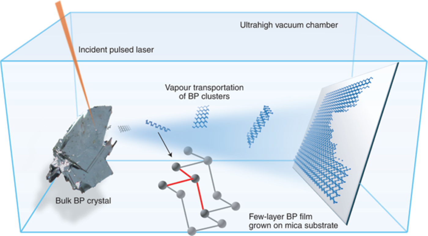
Figure 1. A schematic representation of large-scale BP growth on a mica substrate using pulsed laser deposition
More recently, Prof. Hao’s team introduced a wet transfer method that utilises ethylene-vinyl acetate (EVA) polymer and an ethylene glycol (EG) solution to transfer high-crystalline, large-area PLD-BP films onto SiO2/Si substrates. The results were reported in an article published in Nature Communications [2]. The method is promising for integrating scalable 2D BP thin films into electronic and optoelectronic devices.
The transfer process for large BP thin films is illustrated in Figure 2. After growing the BP film on a mica substrate using PLD, an EVA polymer solution is applied via spin-coating onto the film. To prevent degradation due to oxygen and water, an EG solution is used as the wet medium. The assembly is then immersed in the EG solution at 50 °C for an hour, allowing the EG solution to permeate the interface between the mica and BP film, facilitated by a scratch made at the edge of the film. Once the EVA polymer/BP film is peeled off and attached to a new substrate, any residual EG is evaporated in a vacuum drying oven and the polymer layer is removed using tetrahydrofuran.
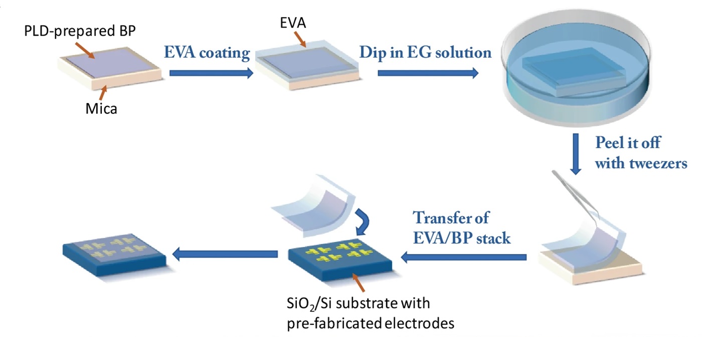
Figure 2. A schematic illustration of the ethylene-vinyl acetate (EVA)-assisted wet transfer process of PLD-prepared BP thin film in ethylene glycol (EG) solution
The successful transfer of large-area BP films relies on the adhesion between the polymer and BP film being stronger than that between the BP and the mica. EVA is selected as the adhesive layer, while EG serves as the transfer solvent, both chosen for their optimal adhesion properties. The polar groups in EVA enhance its adhesion to BP, allowing efficient detachment from the mica. In addition, the use of non-polar EG helps maintain the thickness and adhesion of the EVA layer, thereby facilitating effective transfer of the BP film.
The research team made use of the transferred films to fabricate BP-based bottom-gate field-effect transistor (FET) arrays. They conducted a detailed comparison of BP FETs fabricated through their research [2] with those produced employing other methods as reported in previous studies [1, 3 – 5] (Table 1). In contrast to the direct mechanical exfoliation and liquid exfoliation from high-quality BP bulk crystals, the new large-scale BP preparation process proposed by the research team provides distinct advantages of uniform film, much larger lateral area of 104 µm, and reduced thickness to approximately 5 nm, while utilising the same device structure on silicon substrates. With regard to the device performance, the wet-transferred BP FET demonstrates comparable and even superior characteristics across all aspects, except for a slightly lower on/off ratio when compared to BP FET prepared through chemical vapour deposition (CVD).
Table 1. Comparison of thin-film FETs constructed using BP in different preparation methods
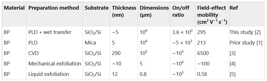
Note: CVD – chemical vapour deposition; PLD – pulsed laser deposition.
The research team further compared the performance of BP with the most representative transition-metal dichalcogenides material, MoS2 in fabricating thin film FETs with the wet transferred method [6 – 8] (Table 2). Comparatively, wet-transferred few-layer BP possesses a much higher carrier mobility (295 cm2V-1s-1) than wet-transferred monolayer MoS2 (ranged from 4.5 to 35cm2V-1s-1), although demonstrating a lower on/off ratio compared to multilayer MoS2. The wet-transferred BP film possesses exceptional properties, such as a larger lateral dimension and much higher field-effect mobility. Notably, the wet-transferred BP FETs exhibit a remarkable level of sensitivity to small changes in the back-gate voltage attributable to the unique material properties of BP. This exceptional sensitivity makes BP very suitable for applications requiring precise control and manipulation of electrical signals, promoting the functionalities and performance of BP in electronic devices and circuits.
Table 2. Comparison of wet-transferred thin-film FETs constructed by BP and MoS2
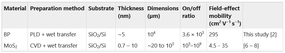
Note: CVD – chemical vapour deposition; PLD – pulsed laser deposition.
The tactical and smart wet transfer approach enables the successful transfer of high-crystalline PLD-grown BP ultrathin films on a centimetre-scale from mica to SiO2/Si substrate. This technique effectively addresses the challenge of producing large-scale, uniform, and continuous 2D ultrathin BP films, while preserving the structural integrity of devices on silicon substrates, which exhibit remarkable electrical characteristics. This methodology holds substantial promise for the future integration of scalable 2D thin films into electronic and optoelectronic devices, highlighting its potential to advance various technological fields.
The research is supported by The Hong Kong Polytechnic University (Grants 1-CE0H and 1-YWBG), the Research Grants Council of Hong Kong (Grants GRF PolyU 15301121, PolyU SRFS2122-5S02, and AoE/P-701/20), and RGC Senior Research Fellowship. The data source is available at: https://www.nature.com/articles/s41467-024-51140-z#Sec11. All raw data generated during the current study are available from the corresponding authors upon request.
Prof. Hao was ranked among the top 2% most-cited scientists worldwide (for career-long) by Stanford University in the field of nanoscience and nanotechnology for five consecutive years from 2020 to 2024. Prof. He was conferred the title “Hong Kong Senior Research Fellow” by the Research Grants Council of Hong Kong in 2021/22. Prof. Hao is currently the Director of Research Centre for Nanoscience and Nanotechnology of The Hong Kong Polytechnic University.
| Note |
|---|
Mechanical exfoliation often results in variations in layer thickness and size, leading to difficulties in controlling the properties of the exfoliated material. Additionally, the process can be labour-intensive and time-consuming, and the inconsistency in the resulting BP flakes can lead to unreliable performance in devices fabricated from these materials.
| References |
|---|
[1] Wu, Z., Lyu, Y., Zhang, Y., Ding, R., Zheng, B., Yang, Z., Lau, S. P., Chen, X. H., & Hao, J. (2021). Large-scale growth of few-layer two-dimensional black phosphorus. Nature Materials, 20(9), 1203–1209. https://doi.org/10.1038/s41563-021-01001-7
[2] Zhao, Y., Mao, J., Wu, Z., Io, W. F., Pang, S.-Y., Zhao, Y., & Hao, J. (2024). A clean transfer approach to prepare centimetre-scale black phosphorus crystalline multilayers on silicon substrates for field-effect transistors. Nature Communications, 15(1), 6795–6798. https://doi.org/10.1038/s41467-024-51140-z
[3] Chen, C., Yin, Y., Zhang, R., Yuan, Q., Xu, Y., Zhang, Y., Chen, J., Zhang, Y., Li, C., Wang, J., Li, J., Fei, L., Yu, Q., Zhou, Z., Zhang, H., Cheng, R., Dong, Z., Xu, X., Pan, A., … He, J. (2023). Growth of single-crystal black phosphorus and its alloy films through sustained feedstock release. Nature Materials, 22(6), 717–724. https://doi.org/10.1038/s41563-023-01516-1
[4] Na, J., Lee, Y. T., Lim, J. A., Hwang, D. K., Kim, G.-T., Choi, W. K., & Song, Y.-W. (2014). Few-Layer Black Phosphorus Field-Effect Transistors with Reduced Current Fluctuation. ACS Nano, 8(11), 11753–11762. https://doi.org/10.1021/nn5052376
[5] Yasaei, P., Kumar, B., Foroozan, T., Wang, C., Asadi, M., Tuschel, D., Indacochea, J. E., Klie, R. F., & Salehi-Khojin, A. (2015). High-Quality Black Phosphorus Atomic Layers by Liquid-Phase Exfoliation. Advanced Materials (Weinheim), 27(11), 1887–1892. https://doi.org/10.1002/adma.201405150
[6] Shen, Y., Wu, Y., Lee, L., Chen, J., Wani, S. S., Yang, T., Luo, C. W., Siao, M., Yu, Y., Chiu, P., & Chueh, Y. (2021). Rational Design on Wrinkle‐Less Transfer of Transition Metal Dichalcogenide Monolayer by Adjustable Wettability‐Assisted Transfer Method. Advanced Functional Materials, 31(45). https://doi.org/10.1002/adfm.202104978
[7] Mondal, A., Biswas, C., Park, S., Cha, W., Kang, S.-H., Yoon, M., Choi, S. H., Kim, K. K., & Lee, Y. H. (2024). Low Ohmic contact resistance and high on/off ratio in transition metal dichalcogenides field-effect transistors via residue-free transfer. Nature Nanotechnology, 19(1), 34–43. https://doi.org/10.1038/s41565-023-01497-x
[8] Lee, C. H., McCulloch, W., Lee, E. W., Ma, L., Krishnamoorthy, S., Hwang, J., Wu, Y., & Rajan, S. (2015). Transferred large area single crystal MoS2 field effect transistors. Applied Physics Letters, 107(19). https://doi.org/10.1063/1.4934941
 | Prof. Jianhua HAO Director of the Research Centre for Nanoscience and Nanotechnology |