Bioinspired In-sensor Computing Architectures and Optimisation in Sensory AI Systems
Other Articles
Bioinspired inventions have led to innovations in more energy-efficient, low-latency, and memory-optimised sensory AI systems.
Study conducted by Prof. Yang CHAI and his research team
Sensory AI are artificial intelligence systems that aim to mimic human sensory perceptions and understandings by equipping machines with the ability to process and interpret data akin to human sensory experiences, such as visual or auditory inputs. Currently, one of the most prevalent forms of sensory input in AI is computer vision, which is pivotal in areas such as image recognition, object detection, and scene understanding. In dynamic motion recognition, high energy consumption and time latency are common challenges when a high volume of analogue signals generated by dynamic vision sensors (DVS) is converted into digital form and then transferred to separate digital processors. Recently, there has been a surge in research into vision pre-processing and artificial neural network (ANN) construction at sensory terminals, which are used for contrast enhancement, noise reduction, visual adaptation, and image recognition. However, in-sensor-based vision computing has mostly been applied to static-image-related tasks, where sensory devices respond to absolute light illumination but lack event-driven characteristics and dynamic-motion detection capabilities.
Drawing inspiration from natural bioinspired sensory systems, a research team led by Yang CHAI, Associate Dean (Research) of the Faculty of Science and a Professor in the Department of Applied Physics at the Hong Kong Polytechnic University, has developed a number of advanced computational hardware for sensory AI systems. These inventions have initiated innovative solutions that epitomise the latest standards of sensory AI, designed to meet the growing demands for energy-efficient, low-latency, and memory-optimised systems, serving as an indispensable foundation for a smart digital society.
Advancing in-sensory computing in dynamic-motion detection
Writing in Nature Nanotechnology, CHAI’s research team fabricated optoelectronic graded neurons, a phototransistor array that mimics the non-spiking graded neurons (retina-lamina) of flying insects to perceive dynamic motions (Figure 1)1. The phototransistors consist of bilayer molybdenum disulfide (MoS2), a semiconductor that captures modulated light signals and converts them into electrical signals, leveraging changes of light intensities and durations over time (Figure 2). The MoS2 phototransistors are designed to contain shallow charge trapping centres at the surface and a local bottom-gate structure, enabling them to process pixel-level temporal sequences and efficiently encode temporal information at sensory terminals, thereby reducing the transfer of abundant vision data by fusing spatiotemporal (spatial and temporal) information within a computation unit. This characteristic enables the phototransistor to achieve an information transmission rate of 1,200 bits per second. The device can capture light stimulation with a frequency of at least 100 Hz, emulating the high flicker function frequency (FFF) vision systems of flying insects to perceive objects with high motion speeds.
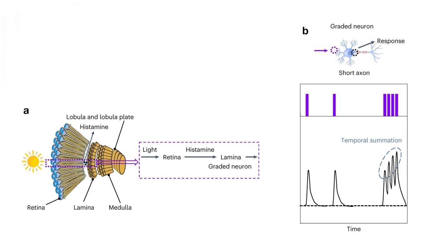
Figure 1. Agile motion perception of the insect visual system.
a, Schematic of the tiny insect visual system. Light stimulation can cause a graded membrane potential in photoreceptors in the retina and the release of histamine, which transfers to the lamina neuron (a typical graded neuron) for temporal processing. The lamina neurons transmit the processed signals to the medulla and lobula layers for action recognition.
b, The structure (top) and response characteristics (bottom) of a graded neuron. A graded neuron can respond to sequential stimulation with nonlinear temporal summation characteristics.
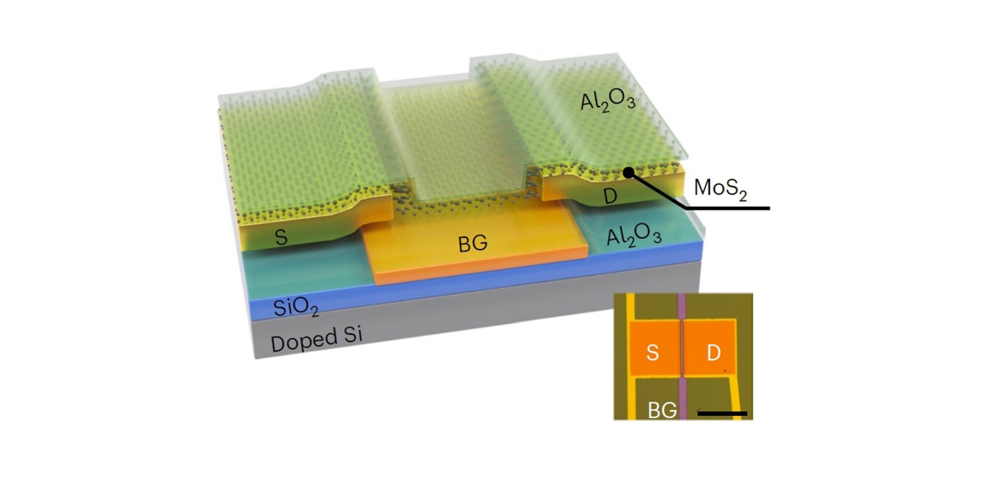
Figure 2. Schematic of the MoS2 phototransistor.
By encoding the spatiotemporal information and feeding the compressed images into an ANN (Figure 3a), the accuracy of action recognition with the phototransistor array reaches 99.2%, significantly higher than that of conventional image sensors (with an accuracy of around 50%). The sensor array is capable of recognising motion with a temporal resolution ranging from 10 ms to 1,000 s, enabling it to encode actions across different timescales, from the slow motion of a snail to the fast motion of a cheetah (Figure 3b). The research addresses challenges in motion processing that demand considerable computational resources, leading to promising potential applications in autonomous vehicles and surveillance systems. This research was chosen as Top Ten Advances in Chinese Chip Science in 2023 by Chip, an international peer-review journal published by Shanghai Jiao Tong University and Elsevier Group.
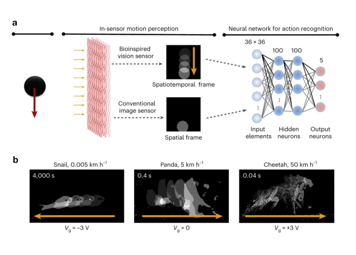
Figure 3. Action recognition based on bioinspired vision sensors and conventional image sensors.
a, A tiny neural network for action recognition with bioinspired vision and conventional image sensors. Bioinspired vision sensors can output spatiotemporal frames, while conventional vision sensors output only spatial frames.
b, The bioinspired photosensors can encode spatiotemporal information at different time scales, covering the motion of snails, pandas and cheetahs with distinctly different moving speeds ranging from 0.005 to 50 km h−1.
In addition, the phototransistors could enhance the image contrast, thus capturing images accurately under varying light illumination. The multiple charge-trap states in the surface enable the sensor to trap or de-trap electrons of the channel under different gate voltages. The processes are controlled by the local gate terminal at the bottom of the sensor, allowing two contrary photoresponses (excitation and inhibition) to be established under background light illumination in the same device (Figure 4). Emulating the human visual adaptability in retina, the sensors are photosensitive across a dynamic range of light illumination up to 199 dB, which is superior to the benchmark AI sensor using silicon complementary metal-oxide with a dynamic range of 70 dB2. After training the phototransistor array with a three-layer ANN, the MoS2 phototransistors achieved an image recognition rate of 96.9% from dim to bright ambience (scotopic adaption) and an image recognition rate of 96.1% from bright to dim ambience (photopic adaption). The research team reported the visual adaptation feature of the MoS2 phototransistors in Nature Electronics3, and it was recognised as one of the top ten innovation and technology news stories in Hong Kong SAR, China in 2022.
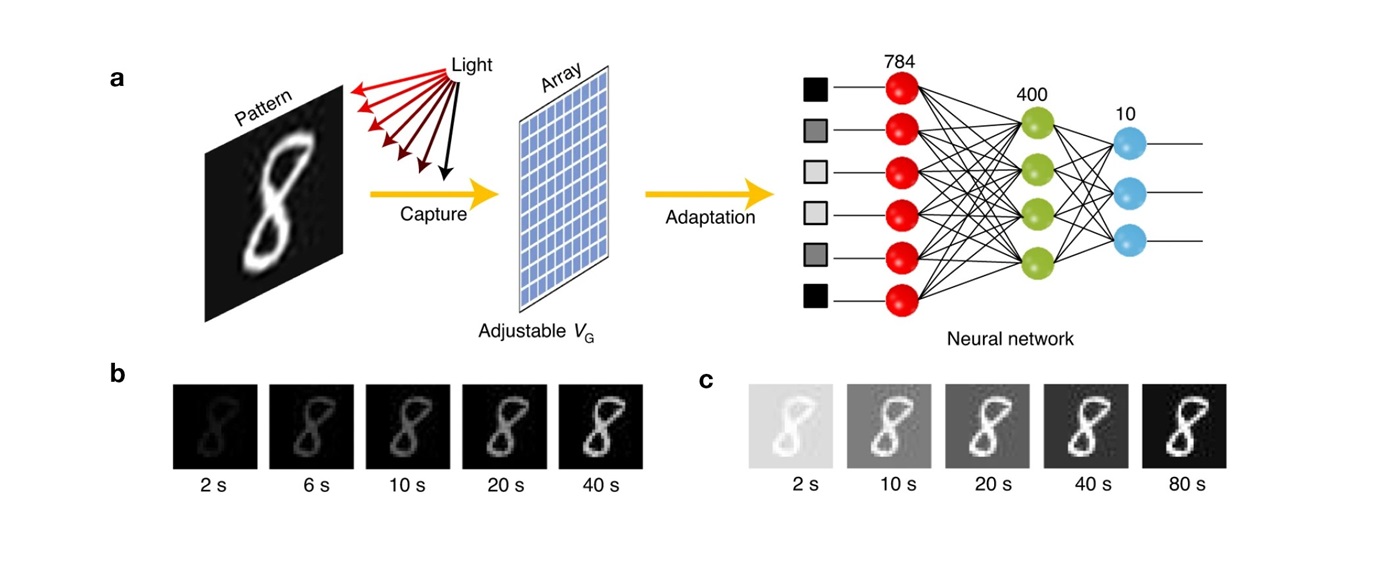
Figure 4. Scotopic and photopic adaptation of MoS2 phototransistor array.
a, Illustration of a machine vision system based on the MoS2 phototransistor array for visual adaptation and an ANN for image recognition.
b,c, Time courses of scotopic (b) and photopic (c) adaptation for the pattern of ‘8’.
Event-driven vision sensors for in-sensory computing
Writing in Nature Electronics, the research team extended their work and investigated a computational vision sensor that combines event-driven sensing with in-sensor computing4. By mimicking spiking neurons in the biological retina, the vision sensor converts dynamic motion into programmable, sparse, and informative spiking signals, forming a spiking neural network (SNN) for motion recognition – an approach that is potentially useful for real-time and energy-efficient machine vision. This innovative device reduces data memory requirement by 98% compared to conventional frame-based sensors.
The research team constructed computational event-driven vision sensors by connecting two floating split-gate photodiodes (made from tungsten diselenide (WSe2)) in parallel, which were configured to generate opposite photocurrents (PN and NP). A capacitor was connected in one of the branches, allowing the two photodiodes to have distinct response time under varying light intensities, resulting in the generation of a spike signal (Figure 5). These sparse signals can efficiently capture motion information, thereby minimising redundant static data. By arranging the photodiode array of vision sensors in a cross-bar configuration, the researchers designed an in-sensor SNN. The vision sensors are trained to emulate synaptic weights, thereby recognising specific input light conditions and generating programmable spikes when light intensity changes. This in-sensor SNN executes computational tasks for motion recognition and achieved 92% accuracy in recognising three distinct types of customised motions after 100 training epochs. By not capturing static vision information, the generated data are largely reduced in the event-driven sensors, improving computation efficiency. With dynamic motion being recognised directly at the sensory terminals, the vision sensor exhibits a fast programming speed of 5μs in an event-driven manner, significantly reducing photo response latency. This approach provides a solid foundation for the development of real-time edge computing vision chips with limited power consumption.
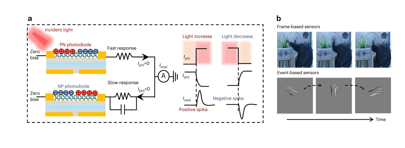
Figure 5. Event-driven in-sensor spiking neural network.
a, Two complementary branches result in zero output photocurrent when the light intensity keeps constant, while the difference of photoresponse time in two branches leads to spike generation upon the change of the light intensity.
b, Comparison between frame- and event-based vision sensors. Frame-based sensors record all pixels at a fixed frame rate, including both the dynamic motion and the static background, while event-based sensors asynchronously capture only the change of light intensity at the local-pixel level.
Drawing from the above research and experiments, the research team has developed novel hardware architectures and optimisation techniques, enabling the deployment of advanced sensory AI systems in mobile devices, Internet of Thing (IoT) sensors, and edge computing, thereby transforming applications in smart cities, autonomous vehicles, and industrial automation. Furthermore, the in-sensor computing strategy has sparked progress in improving decision-making and situational awareness, strengthening privacy and security, and enhancing intelligent automation. For his exceptional contributions, CHAI has been awarded the prestigious title of 2024 winner of the Falling Walls Science Breakthroughs Award in the Engineering & Technology category for “Breaking the Wall of Efficient Sensory AI Systems”5, as well as the Bank of China (Hong Kong) Limited (BOCHK) Science and Technology Innovation Prize 2024 (Artificial Intelligence and Robotics), recognising his development of novel hardware architectures and optimisation techniques for sensory AI.
| References |
|---|
1. Chen, J., Zhou, Z., Kim, B. J., Zhou, Y., Wang, Z., Wan, T., Yan, J., Kang, J., Ahn, J. H., & Chai, Y. (2023). Optoelectronic graded neurons for bioinspired in-sensor motion perception. Nature Nanotechnology, 18(8), 882–888. https://doi.org/10.1038/s41565-023-01379-2
2. Ohta, J. (2020). Smart CMOS image sensors and applications (Second edition.). CRC Press.
3. Liao, F., Zhou, Z., Kim, B. J., Chen, J., Wang, J., Wan, T., Zhou, Y., Hoang, A. T., Wang, C., Kang, J., Ahn, J. H., & Chai, Y. (2022). Bioinspired in-sensor visual adaptation for accurate perception. Nature Electronics, 5(2), 84–91. https://doi.org/10.1038/s41928-022-00713-1
4. Zhou, Y., Fu, J., Chen, Z., Zhuge, F., Wang, Y., Yan, J., Ma, S., Xu, L., Yuan, H., Chan, M., Miao, X., He, Y., & Chai, Y. (2023). Computational event-driven vision sensors for in-sensor spiking neural networks. Nature Electronics, 6(11), 870–878. https://doi.org/10.1038/s41928-023-01055-2
5. Falling Walls Foundation. (2024, September 12). Breaking Barriers in Sensory AI: Yang Chai’s Energy-Efficient Innovations [Press release].
https://falling-walls.com/breaking-barriers-sensory-ai-yang-chais-energy-efficient-innovations
 | Prof. Yang CHAI Associate Dean (Research) of the Faculty of Science and Professor in the Department of Applied Physics |


